
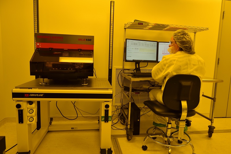
 The Heidelberg Direct Write Lithography system is a flexible, high resolution photolithography tool for direct writing. The MLA100 automatically detects the perimeter of the sample and uses a digital mask to sequentially expose smaller pattern fields to yield a unified design.
Key Features
- Minimum feature size down to 1 µm
- Non-contact exposure
- Substrates up to 5” x 5”
- Light source at 365nm
- Alignment accuracy of 500nm
- Multiple data input formats
Key Applications and available processes
Fast patterning of masks and wafers in Life Science, MEMS, Micro-Optics, Semiconductor, Sensors, Actuators, Materials Research
Check Availability
Already have an account?
Reserve this tool with FOM.
Equipment Fee
Fabrication Service 2
Core Facility
Gertrude E. and John M. Petersen Institute of NanoScience and Engineering
Location
Lower Campus
Equipment Type
Lithography